Fast and Energy-efficient Photonic Integrated Circuits Powered by On-chip Lasers for Artificial Intelligence Models

Project Details
Program
Electrical and Computer Engineering
Field of Study
Photonics, Physics, Semiconductors
Division
Computer, Electrical and Mathematical Sciences and Engineering
Faculty Lab Link
Project Description
The rise of AI-driven services has triggered a significant increase in the demand for both processing capacity and energy efficiency. Currently, the performance of electronic processors is limited by power dissipation, integration density, and clock speed, especially for matrix-vector multiplication (MVM), which comprises more than 80% of the operations in modern AI models.
In contrast, optical neural networks (ONNs) provide a promising alternative by exploiting intrinsic photon properties to calculate MVM, offering ultra-high bandwidth and processing frequency (>100GHz), ultra-low power consumption (sub-pJ/bit), and high parallelism through additional dimension division multiplexing. Silicon photonics, with its advantages of CMOS compatible manufacturability and high-density integration capacity, stands out as a promising platform for the realization of ONNs. However, the inherent indirect bandgap of silicon has hindered the progress of on-chip light sources compared to other photonic devices, creating a significant bottleneck for industrial-scale production.
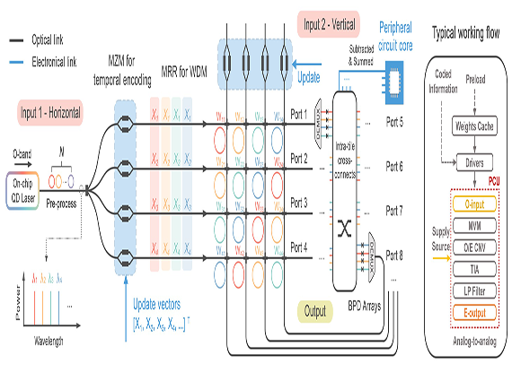
Leveraging Intel’s silicon photonics platform, our team earlier has led the integration of quantum dot (QD) lasers with silicon photonic integrated circuits (PICs). In this project, we aim to further develop a volume-manufacturable, fully integrated ONN system with high bandwidth and energy efficiency. This is in contrast to the bulky off-chip solution that requires ~(2dB+6dB) power in coupling and modulation alone. A key component of this system is the compact, energy-efficient, and robust QD laser source, which will be achieved via efficient coupling to planar waveguides, optical modulators, buffers, and wavelength multiplexers in the Si-on-insulator PIC platform.
After addressing critical challenges in on-chip light sources, we will co-design hardware and software for a fully integrated ONN system. We propose a crossbar architecture utilizing micro-ring arrays, which maximizes on-chip laser benefits by offering compactness and high parallelism. Simulations of our preliminary ONN model have demonstrated over 91% recognition accuracy on the Modified National Institute of Standards (MNIST) dataset with an overall system computational density exceeding 0.27 TOPS/mm2. Leveraging a 65 nm standard CMOS process line at Intel and the on-chip non-volatile memory, we anticipate an experimental enhancement in computational density by over 70x compared to Google’s TPU accelerator, with a theoretical minimum power consumption reduction of over 1000x.
About the Researcher
Yating Wan
Assistant Professor, Electrical and Computer Engineering
Affiliations
Education Profile
- Postdoc fellow, University of California, Santa Barbara, 2017-2022
- Ph.D. Hong Kong University of Science and Technology, 2017
- B.S. Zhejiang University, 2012
Research Interests
Professor Yating Wana€˜s research interests are in Silicon Photonics with special emphasis on integration of on-chip light sources for short-reach communication links. She is also interested in other related applications including biosensors/bioimaging, energy harvesting, machine vision, and quantum information processing.Selected Publications
- Y. Wan, C. Xiang, J. Guo, R. Koscica, MJ Kennedy, J. Selvidge, Z. Zhang, L. Chang, W. Xie, D.Huang, A. C. Gossard, and J. E. Bowers*, a€œHigh speed evanescent quantum-dot lasers on Sia€, Laser & Photonics Reviews 2100057, 2021.
- Y. Wan, J. Norman, Y. Tong, MJ Kennedy, W. He, J. Selvidge, C. Shang, M. Dumont, A. Malik, H. K. Tsang, A. C. Gossard, and J. E. Bowers*, a€œ1.3 Aµm quantum-dot distributed feedback lasers directly grown on (001) Sia€, Laser & Photonics Reviews. 14 (7), 2070042, 2020.
- Y. Wan, C. Shang, J. Huang, Z. Xie, A. Jain, D. Inoue, B. Chen, J. Norman, A. C. Gossard, and J. E. Bowers*, a€œLow-dark current 1.55 I¼m InAs quantum dash waveguide photodiodesa€, ACS nano 14(3), 3519-3527, 2020.
- Y. Wan, S. Zhang, J. Norman, MJ Kennedy, W. He, Y. Tong, C. Shang, J. He, H. K. Tsang, A. C. Gossard, and J. E. Bowers*, a€œDirectly modulated single-mode tunable quantum dot lasers at 1.3 Aµma€, Laser & Photonics Reviews. 14(3), 1900348, 2020
- Y. Wan, S. Zhang, J. Norman, MJ Kennedy, W. He, S. Liu, C. Xiang, C. Shang, J. He, A. C. Gossard, and J. E. Bowers*, a€œTunable quantum dot lasers directly grown on Sia€, Optica, 6(11), 1394-1400 (2019).
Desired Project Deliverables
The students are expected to acquire the basic knowledge of the design of the integrated silicon photonics chips, proficient skills of device designs using simulation tools, hand-on experimental experiences of optoelectronic device characterizations, and conference/journal publications.
Recommended Student Background
Semiconductor physics
Optical computing
Integrated photonics
Semiconductor lasers
We are shaping the
World of Research
Be part of the journey with VSRP
3-6 months
Internship period
100+
Research Projects
3.5/4
Cumulative GPA
310
Interns a Year